Texas Instruments LMX1214 Bruksanvisning
Texas Instruments ej kategoriserat LMX1214
Läs gratis den bruksanvisning för Texas Instruments LMX1214 (49 sidor) i kategorin ej kategoriserat. Guiden har ansetts hjälpsam av 6 personer och har ett genomsnittsbetyg på 4.2 stjärnor baserat på 2 recensioner. Har du en fråga om Texas Instruments LMX1214 eller vill du ställa frågor till andra användare av produkten? Ställ en fråga
Sida 1/49
LMX1214 Low-Noise, High-Frequency Buffer and Divider
1 Features
•Clock buffer for 300MHz to 18GHz frequency
•Divider output frequency supported up to 8GHz
•Ultra-Low Noise
–Noise floor of –161dBc/Hz at 6GHz output
–36fs additive jitter (100Hz to f
CLK
) at 6GHz
output
–5fs additive jitter (100Hz - 100MHz)
•4 high-frequency clocks output
–with shared divider by 1 (Bypass), 2, 3, 4, 5, 6,
7, and 8
•1ps typical output to output skew
•Support pin mode options for outputs enable and
divider /2, /3 and /4 values set
•AUXCLK output
–On separate divide bank
–1, 2, 4 pre-divider
–1 (bypass), 2, …, 1023 post divider
•8 programmable output power levels
•SYNC feature to all divides
•2.5V operating voltage
•–40ºC to +85ºC operating temperature
2 Applications
•Test & Measurement:
–Oscilloscope
–Wireless equipment testers
–Wideband digitizers
•Aerospace & Defense:
–Radar
–Electronic warfare
–Seeker Front end
–Munitions
–Phase array antenna / Beam forming
•General Purpose:
–Data converter clocking
–Clock buffer distribution / division
3 Description
The LMX1214 features high output frequency, ultra-
low noise floor, and very low skew clocks distribution.
The device has four high-frequency output clocks
and a lower frequency auxiliary clock output. The
device supports both buffer and divide mode for the
high-frequency clocks. This device can distribute the
mutlichannel, low skew, ultra-low noise local oscillator
signals to multiple mixers.
Package Information
PART NUMBERPACKAGE
(1)
PACKAGE SIZE
(2)
LMX1214RHA (VQFN, 40)6mm × 6mm
(1)For all available packages, see the orderable addendum at
the end of the data sheet.
(2)The package size (length × width) is a nominal value and
includes pins, where applicable.
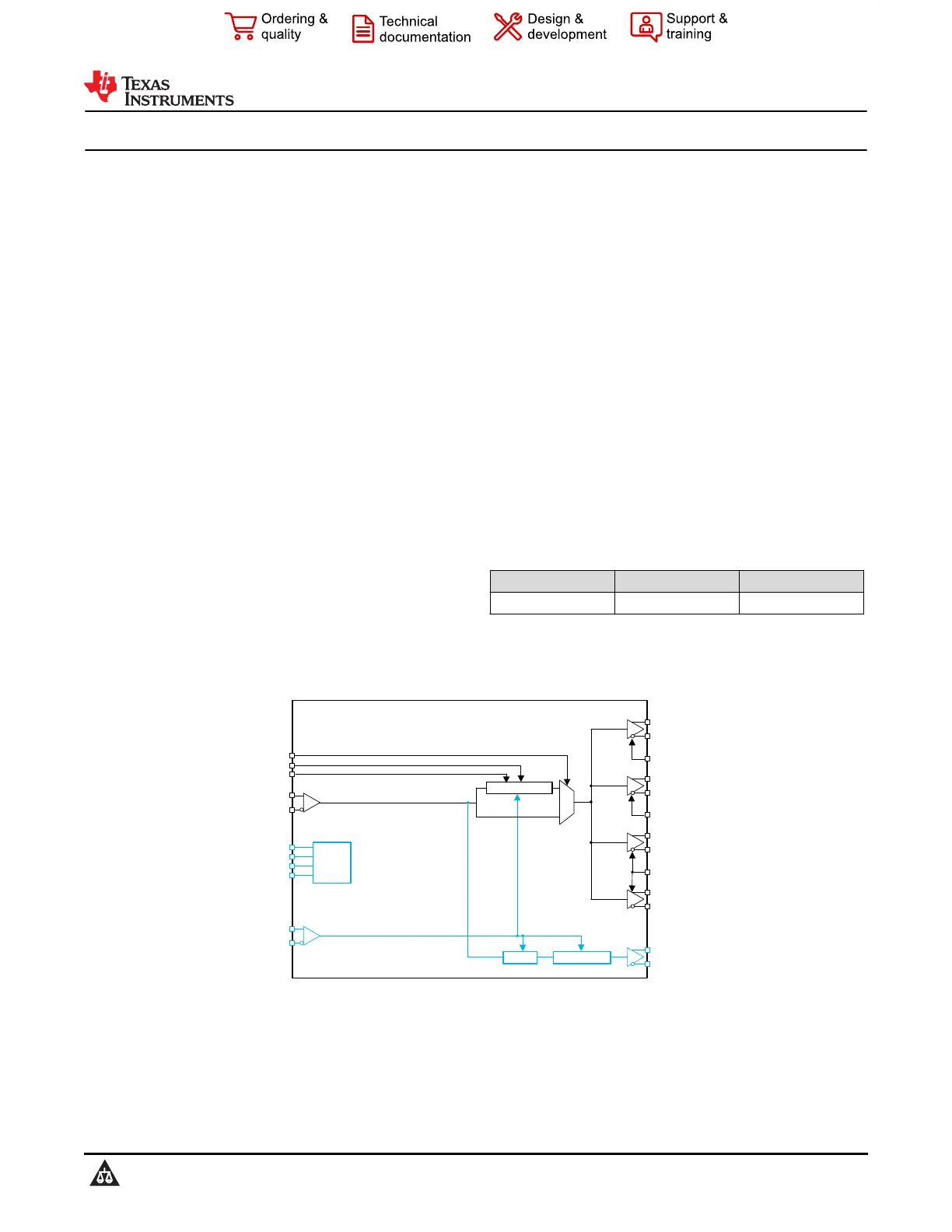
CLKOUT0
CLKOUT1
CLKOUT2
CLKOUT3
AUXCLKOUT
CLKIN
SYNC
÷1,2,3,...1023
Digital
Control
SDI
CS#
MUXOUT
SCK
÷1,2,4
CLK0_EN
CLK1_EN
CLK23_EN
Pin Control:
Buffer Mode
Divide with 2,3,4
Output Enables
SPI Control:
AUXCLKOUT
Divide with 5,6,7,8
Phase SYNC
Ouput Power Control
DIV_SEL0
DIV_SEL1
MUXSEL
÷2,3,4,5,6,7,8
Legend
Accessible through SPI control only
Accessible with Pin and SPI control
Block Diagram
LMX1214
SNAS866A – DECEMBER 2023 – REVISED SEPTEMBER 2024
An IMPORTANT NOTICE at the end of this data sheet addresses availability, warranty, changes, use in safety-critical applications,
intellectual property matters and other important disclaimers. PRODUCTION DATA.
Produktspecifikationer
| Varumärke: | Texas Instruments |
| Kategori: | ej kategoriserat |
| Modell: | LMX1214 |
Behöver du hjälp?
Om du behöver hjälp med Texas Instruments LMX1214 ställ en fråga nedan och andra användare kommer att svara dig
ej kategoriserat Texas Instruments Manualer

3 April 2026
31 Mars 2026
5 Mars 2026
5 Mars 2026
5 Mars 2026
5 Mars 2026
5 Mars 2026
5 Mars 2026
5 Mars 2026
5 Mars 2026
ej kategoriserat Manualer
Nyaste ej kategoriserat Manualer
3 April 2026
3 April 2026
3 April 2026
3 April 2026
3 April 2026
3 April 2026
3 April 2026
3 April 2026
3 April 2026