Texas Instruments LMK3C0105-Q1 Bruksanvisning
Texas Instruments ej kategoriserat LMK3C0105-Q1
Läs gratis den bruksanvisning för Texas Instruments LMK3C0105-Q1 (55 sidor) i kategorin ej kategoriserat. Guiden har ansetts hjälpsam av 8 personer och har ett genomsnittsbetyg på 4.4 stjärnor baserat på 2 recensioner. Har du en fråga om Texas Instruments LMK3C0105-Q1 eller vill du ställa frågor till andra användare av produkten? Ställ en fråga
Sida 1/55
LMK3C0105-Q1 Reference-less 5-LVCMOS-Output Programmable BAW Clock
Generator
1 Features
•AEC-Q100 Grade 2 qualified for automotive
applications
•Ambient Temperature: –40°C to 105°C
•Functional Safety-Capable:
–Documentation available to aid functional safety
system design
•Integrated BAW resonator, no need for external
reference
•Flexible frequency generation:
–1.8V/2.5V/3.3V LVCMOS outputs supported up
to 200MHz
–Dual Fractional Output Dividers (FODs)
–Up to three unique output frequencies from
2.5MHz to 200MHz
•Example: OUTA/B/C/D/E = 25MHz
•Example: OUTA/B = 100MHz, OUTC/D =
50MHz, OUTE = 25MHz
–Generation of up to 5 LVCMOS clocks on
OUTA through OUTE pins
•Total output frequency stability: ±25ppm
•2 functional modes: I2C or preprogrammed OTP
•Mixed SSC and non-SSC output support
•Programmable SSC modulation depth
–Preprogrammed: –0.1%, –0.25%, –0.3%,
and –0.5% down spread
–Register programmable: –0.1% to –3% down
spread or ±0.05% to ±1.5% center spread
•1.8V to 3.3V supply voltage
•Start-up time: <5ms
•Output skew: <50ps (outputs from the same FOD)
•Fail-safe input and VDD pins
2 Applications
•Crystal replacement (up to 5 single-ended clocks)
•ASIC, FPGA, MCU reference clocking
•Advanced Driver Assistance Systems (ADAS)
•High-Performance Compute
•Head Unit & Digital Cockpit
•Vehicle Instrument Cluster
3 Description
The LMK3C0105-Q1 is a 5-output reference-less
clock generator with SSC support. The device is
based on TI proprietary Bulk Acoustic Wave (BAW)
technology and provides ±25ppm clock outputs
without any crystal or external clock reference.
The device can provide 5 SSC clocks, 5 non-SSC
clocks, or a mix of SSC and non-SSC clocks
at the same time. Up to three different output
frequencies can be generated across the five outputs.
Each output channel can select either FOD as the
frequency source to generate four LVCMOS clocks;
the REF_CTRL pin functions as a fifth LVCMOS clock
output, and can select either FOD as the source.
The device can be easily configured through either
pins or the I
2
C interface. An external DC/DC can be
used to power the device. Refer to Power Supply
Recommendationsfor detailed guidelines on power
supply filtering and sourcing from a DC/DC supply.
Package Information
PART NUMBERPACKAGE
(1)
PACKAGE SIZE
(2)
LMK3C0105-Q1RGT (VQFN,16)3.0mm × 3.0mm
(1)For more information, see Section 12.
(2)The package size (length × width) is a nominal value and
includes pins, where applicable.
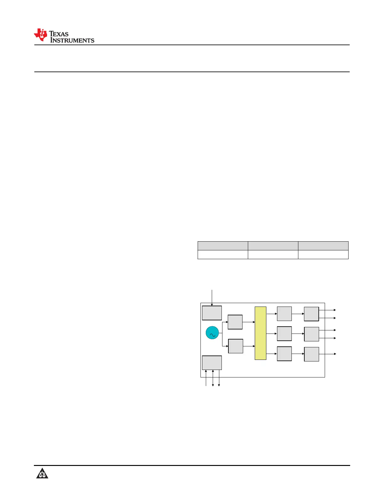
FOD1
BAW
FOD0
Clock
Dist
Output
Buffer
LMK3C0105
High performance reference-less clock generator
Power
Conditioning
Interface
I2C/OTP
Output
Divider
Output
Buffer
Output
Divider
OUTA
OUTB
OUTC
OUTD
Output
Buffer
REF_CLK
Divider
OUTE
Simplified Block Diagram
LMK3C0105-Q1
SNAS881B – APRIL 2025 – REVISED OCTOBER 2025
An IMPORTANT NOTICE at the end of this data sheet addresses availability, warranty, changes, use in safety-critical applications,
intellectual property matters and other important disclaimers. PRODUCTION DATA.
Produktspecifikationer
| Varumärke: | Texas Instruments |
| Kategori: | ej kategoriserat |
| Modell: | LMK3C0105-Q1 |
Behöver du hjälp?
Om du behöver hjälp med Texas Instruments LMK3C0105-Q1 ställ en fråga nedan och andra användare kommer att svara dig
ej kategoriserat Texas Instruments Manualer

3 April 2026
31 Mars 2026
5 Mars 2026
5 Mars 2026
5 Mars 2026
5 Mars 2026
5 Mars 2026
5 Mars 2026
5 Mars 2026
5 Mars 2026
ej kategoriserat Manualer
Nyaste ej kategoriserat Manualer
3 April 2026
3 April 2026
3 April 2026
3 April 2026
3 April 2026
3 April 2026
3 April 2026
3 April 2026
3 April 2026