Microchip PIC24HJ64GP510 Bruksanvisning

Microchip Inte kategoriserad PIC24HJ64GP510

Läs nedan 📖 manual på svenska för Microchip PIC24HJ64GP510 (84 sidor) i kategorin Inte kategoriserad. Denna guide var användbar för 6 personer och betygsatt med 4.5 stjärnor i genomsnitt av 2 användare

Sida 1/84
© 2010 Microchip Technology Inc. DS70152H-page 1
dsPIC33F/PIC24H
1.0 DEVICE OVERVIEW
This document defines the programming specification
for the dsPIC33F 16-bit Digital Signal Controller (DSC)
and PIC24H 16-bit Microcontroller (MCU) families. This
programming specification is required only for those
developing programming support for the dsPIC33F/
PIC24H family. Customers using only one of these
devices should use development tools that already
provide support for device programming.
Topics covered include:
1.0 Device Overview ......................................................... 1
2.0 Programming Overview of the dsPIC33F/PIC24H ...... 1
3.0 Device Programming – Enhanced ICSP ..................... 8
4.0 The Programming Executive ..................................... 19
5.0 Device Programming – ICSP .................................... 28
6.0 Programming the Programming Executive
to Memory ................................................................. 45
7.0 Device ID................................................................... 50
8.0 AC/DC Characteristics and Timing Requirements .... 54
Appendix A: Hex File Format .............................................. 57
Appendix B: Device ID Register Silicon Errata Addendum . 58
Appendix C: Diagnostic and Calibration Registers ............. 59
Appendix D: Checksum Computation ................................. 61
Appendix E: Revision History.............................................. 74
2.0 PROGRAMMING OVERVIEW
OF THE dsPIC33F/PIC24H
There are two methods of programming the dsPIC33F/
PIC24H family of devices discussed in this
programming specification. They are:
In-Circuit Serial Programming™ (ICSP™)
programming capability
Enhanced In-Circuit Serial Programming
The ICSP programming method is the most direct
method to program the device; however, it is also the
slower of the two methods. It provides native, low-level
programming capability to erase, program and verify
the chip.
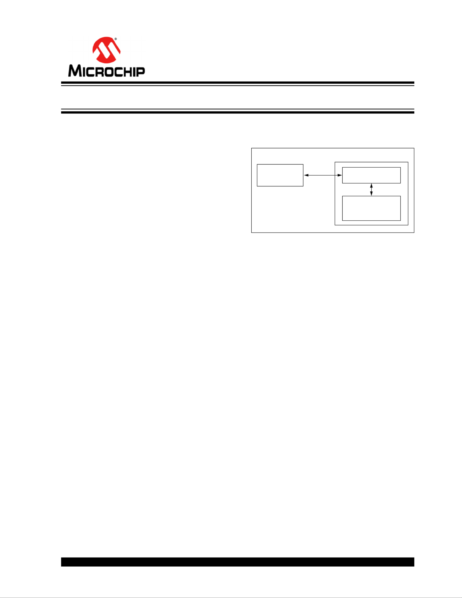
The Enhanced ICSP protocol uses a faster method that
takes advantage of the programming executive, as
illustrated in . The programming executiveFigure 2-1
provides all the necessary functionality to erase,
program and verify the chip through a small command
set. The command set allows the programmer to
program the dsPIC33F/PIC24H Programming
Specification devices without having to deal with the
low-level programming protocols of the chip.
FIGURE 2-1: PROGRAMMING SYSTEM
OVERVIEW FOR
ENHANCED ICSP™
This specification is divided into major sections that
describe the programming methods independently.
Section 3.0 “Device Programming Enhanced
ICSP” describes the Enhanced ICSP method.
Section 5.0 “Device Programming ICSP”
describes the ICSP method.
2.1 Power Requirements
All devices in the dsPIC33F/PIC24H family are dual
voltage supply designs: one supply for the core and
another for the peripherals and I/O pins. A regulator is
provided on-chip to alleviate the need for two external
voltage supplies.
All of the dsPIC33F/PIC24H devices power their core
digital logic at a nominal 2.5V. To simplify system
design, all devices in the dsPIC33F/PIC24H
Programming Specification family incorporate an
on-chip regulator that allows the device to run its core
logic from VDD.
The regulator provides power to the core from the other
VDD pins. A low-ESR capacitor (such as tantalum) must
be connected to the VCAP pin (Figure 2-2). This helps
to maintain the stability of the regulator. The
specifications for core voltage and capacitance are
listed in Section 8.0 “AC/DC Characteristics and
Timing Requirements”.
dsPIC33F/PIC24H
Programmer Programming
Executive
On-Chip Memory
dsPIC33F/PIC24H Flash Programming Specification
dsPIC33F/PIC24H PROGRAMMING SPECIFICATION
DS70152H-page 2 © 2010 Microchip Technology Inc.
FIGURE 2-2: CONNECTIONS FOR THE
ON-CHIP REGULATOR
2.2 Program Memory Write/Erase
Requirements
The program Flash memory on the dsPIC33F/PIC24H
has a specific write/erase requirement that must be
adhered to, for proper device operation. The rule is that
any given word in memory must not be written without
first erasing the page in which it is located. Thus, the
easiest way to conform to this rule is to write all the data
in a programming block within one write cycle. The
programming methods specified in this document
comply with this requirement.
2.3 Pins Used During Programming
The pins that are used for programming are listed in
Table 2-1.
TABLE 2-1: PINS USED DURING PROGRAMMING
Note 1: These are typical operating voltages. Refer
to TABLE 8-1: “AC/DC Characteristics
and Timing Requirements” for the full
operating ranges of VDD and VCAP.
2: It is important for the low-ESR capacitor to
be placed as close as possible to the V
CAP
pin.
VDD
VCAP
VSS
dsPIC33F/PIC24H
CEFC
3.3V
Note: A program memory word can be
programmed twice before an erase, but
only if (a) the same data is used in both
program operations or (b) bits containing
1’ are set to ‘0’ but no0’ is set to 1’.
Note: Refer to the specific device data sheet for
complete pin diagrams of the dsPIC33F/
PIC24H devices.
Pin Name
During Programming
Pin Name Pin Type Pin Description
MCLR MCLR P Programming Enable
VDD and AVDD(1) VDD P Power Supply
VSS and AVSS(1) VSS P Ground
VCAP CAPV P CPU Logic Filter Capacitor Connection
PGEC1 PGEC1 I Primary Programming Pin Pair: Serial Clock
PGED1 PGED1 I/O Primary Programming Pin Pair: Serial Data
PGEC2 PGEC2 I Secondary Programming Pin Pair: Serial Clock
PGED2 PGED2 I/O Secondary Programming Pin Pair: Serial Data
PGEC3 PGEC3 I Tertiary Programming Pin Pair: Serial Clock
PGED3 PGED3 I/O Tertiary Programming Pin Pair: Serial Data
Legend: I = Input O = Output P = Power
Note 1: All power supply and ground pins must be connected, including analog supplies (AVDD) and ground
(AV ).SS
© 2010 Microchip Technology Inc. DS70152H-page 3
dsPIC33F/PIC24H PROGRAMMING SPECIFICATION
2.4 Memory Map
The program memory map extends from 0x0 to
0xFFFFFE. Code storage is located at the base of the
memory map and supports up to 88K instructions
(about 256 Kbytes). Table 2-2 shows the program
memory size and number of erase and program blocks
present in each device variant. Each erase block or
page contains 512 instructions and each program block
or row, contains 64 instructions.
Locations 0x800000 through 0x800FFE are reserved
for executive code memory. This region stores the
programming executive and the debugging
executive. The programming executive is used for
device programming and the debug executive is
used for in-circuit debugging. This region of memory
cannot be used to store user code.
Locations 0xF80000 through 0xF80017 are reserved
for the device Configuration registers.
Locations 0xFF0000 and 0xFF0002 are reserved for
the Device ID Word registers. These bits can be used
by the programmer to identify which device type is
being programmed. They are described in Section 7.0
“Device ID”. The Device ID registers read out
normally, even after code protection is applied.
Figure 2-3 illustrates the memory map for the
dsPIC33F/PIC24H family variants.
TABLE 2-2: CODE MEMORY SIZE
dsPIC33F/PIC24H Device
User Memory Address
Limit
(Instruction Words)
Write Blocks Erase Blocks
Executive Memory
Address Limit
(Instruction Words)
dsPIC33FJ06GS101 0x000FFE (2K) 32 4 0x8007FE (1K)
dsPIC33FJ06GS102 0x000FFE (2K) 32 4 0x8007FE (1K)
dsPIC33FJ06GS202 0x000FFE (2K) 32 4 0x8007FE (1K)
dsPIC33FJ16GS402 0x002BFE (6K) 88 11 0x8007FE (1K)
dsPIC33FJ16GS404 0x002BFE (6K) 88 11 0x8007FE (1K)
dsPIC33FJ16GS502 0x002BFE (6K) 88 11 0x8007FE (1K)
dsPIC33FJ16GS504 0x002BFE (6K) 88 11 0x8007FE (1K)
dsPIC33FJ12GP201 0x001FFE (4K) 64 8 0x8007FE (1K)
dsPIC33FJ12GP202 0x001FFE (4K) 64 8 0x8007FE (1K)
dsPIC33FJ16GP304 0x002BFE (6K) 88 11 0x800FFE (2K)
dsPIC33FJ32GP202 0x0057FE (11K) 176 22 0x800FFE (2K)
dsPIC33FJ32GP204 0x0057FE (11K) 176 22 0x800FFE (2K)
dsPIC33FJ32GP302 0x0057FE (11K) 176 22 0x800FFE (2K)
dsPIC33FJ32GP304 0x0057FE (11K) 176 22 0x800FFE (2K)
dsPIC33FJ64GP202 0x00ABFE (22K) 344 43 0x800FFE (2K)
dsPIC33FJ64GP204 0x00ABFE (22K) 344 43 0x800FFE (2K)
dsPIC33FJ64GP206 0x00ABFE (22K) 344 43 0x800FFE (2K)
dsPIC33FJ64GP306 0x00ABFE (22K) 344 43 0x800FFE (2K)
dsPIC33FJ64GP310 0x00ABFE (22K) 344 43 0x800FFE (2K)
dsPIC33FJ64GP706 0x00ABFE (22K) 344 43 0x800FFE (2K)
dsPIC33FJ64GP708 0x00ABFE (22K) 344 43 0x800FFE (2K)
dsPIC33FJ64GP710 0x00ABFE (22K) 344 43 0x800FFE (2K)
dsPIC33FJ64GP802 0x00ABFE (22K) 344 43 0x800FFE (2K)
dsPIC33FJ64GP804 0x00ABFE (22K) 344 43 0x800FFE (2K)
dsPIC33FJ128GP202 0x0157FE (44K) 688 86 0x800FFE (2K)
dsPIC33FJ128GP204 0x0157FE (44K) 688 86 0x800FFE (2K)
dsPIC33FJ128GP206 0x0157FE (44K) 688 86 0x800FFE (2K)
dsPIC33FJ128GP306 0x0157FE (44K) 688 86 0x800FFE (2K)
dsPIC33FJ128GP310 0x0157FE (44K) 688 86 0x800FFE (2K)
dsPIC33FJ128GP706 0x0157FE (44K) 688 86 0x800FFE (2K)
dsPIC33FJ128GP708 0x0157FE (44K) 688 86 0x800FFE (2K)
© 2010 Microchip Technology Inc. DS70152H-page 7
dsPIC33F/PIC24H PROGRAMMING SPECIFICATION
FIGURE 2-3: PROGRAM MEMORY MAP
User Memory
Space
0x000000
Configuration Registers
Code Memory
0x02AC00
0x02ABFE
Configuration Memory
Space
(87552 x 24-bit)
0x800000
0xF80000
(12 x 8-bit) 0xF80016
0xF80018
Device ID
0xFEFFFE
0xFF0000
0xFFFFFE
Reserved
0xF7FFFE
Reserved
0x800FFE
0x801000
Executive Code Memory
0x7FFFFE
Reserved
0xFF0002
0xFF0004
Reserved
(2 x 16-bit)
Note: The address boundaries for user Flash and Executive code memory are device dependent.
User Flash
(2048 x 24-bit)
© 2010 Microchip Technology Inc. DS70152H-page 9
dsPIC33F/PIC24H PROGRAMMING SPECIFICATION
3.2 Confirming the Presence of the
Programming Executive
Before programming, the programmer must confirm
that the programming executive is stored in executive
memory. The procedure for this task is illustrated in
Figure 3-2.
First, ICSP mode is entered. Then, the unique
Application ID Word stored in executive memory is read.
If the programming executive is resident, the correct
Application ID Word is read and programming can
resume as normal. However, if the Application ID Word is
not present, the programming executive must be
programmed to executive code memory using the
method described in Section 6.0 “Programming the
Programming Executive to Memory”. See Table 7-1
for the Application ID of each device.
Section 5.0 “Device Programming ICSP” describes
the ICSP programming method. Section 5.11 Reading
the Application ID Word” describes the procedure for
reading the Application ID Word in ICSP mode.
FIGURE 3-2: CONFIRMING PRESENCE
OF PROGRAMMING
EXECUTIVE
3.3 Entering Enhanced ICSP Mode
As illustrated in Figure 3-3, entering Enhanced ICSP
Program/Verify mode requires three steps:
1. The MCLR pin is briefly driven high then low.
2. A 32-bit key sequence is clocked into PGDx.
3. MCLR is then driven high within a specified
period of time and held.
The programming voltage applied to MCLR is VIH,
which is essentially VDD in case of dsPIC33F/PIC24H
devices. There is no minimum time requirement for
holding at V IH. After VIH is removed, an interval of at
least P18 must elapse before presenting the key
sequence on PGDx.
The key sequence is a specific 32-bit pattern,
‘0100 1101 0100 0011 0100 1000 0101 0000’
(more easily remembered as 0x4D434850 in
hexadecimal format). The device will enter Program/
Verify mode only if the key sequence is valid. The Most
Significant bit (MSb) of the most significant nibble must
be shifted in first.
Once the key sequence is complete, V IH must be
applied to MCLR and held at that level for as long as
Program/Verify mode is to be maintained. An interval
time of at least P19 and P7 must elapse before
presenting data on PGDx. Signals appearing on PGDx
before P7 has elapsed will not be interpreted as valid.
On successful entry, the program memory can be
accessed and programmed in serial fashion. While in
the Program/Verify mode, all unused I/Os are placed in
the high-impedance state.
Is
Start
Enter ICSP™ Mode
Application ID
present? (1)
Yes
No
Application ID
Check the
be Programmed
Prog. Executive must
by reading Address
0x8007F0
End
Exit ICSP Mode
Enter Enhanced
Sanity Check
Note 1: See TABLE 7-1: “Device IDs and Revi-
sion” for the Application ID of each
device.
ICSP Mode
Note: When programming a device without
Peripheral Pin Select (PPS) and in
Enhanced ICSP mode, the SPI output pin
(SDOx) may toggle while the device is
being programmed.
© 2010 Microchip Technology Inc. DS70152H-page 15
dsPIC33F/PIC24H PROGRAMMING SPECIFICATION
HPOL FPOR Motor Control PWM High-Side Polarity bit
1 = PWM module high-side output pins have active-high output polarity
0 = PWM module high-side output pins have active-low output polarity
LPOL FPOR Motor Control PWM Low-Side Polarity bit
1 = PWM module low-side output pins have active-high output polarity
0 = PWM module low-side output pins have active-low output polarity
ALTI2C FPOR Alternate I 2C™ pins
1 = I2C mapped to SDA1/SCL1 pins
0 = I2C mapped to ASDA1/SACL1 pins
ALTQIO FPOR Enable Alternate QEI pins
1 = QEA1A, AEB1A and INDX1A are selected as inputs to QEI1
0 = QEA1, AEB1 and INDX1 are selected as inputs to QEI1
ALTSS1 FPOR Enable Alternate SS1 pins
1 = SS1A is selected as I/O to SPI1
0 = SS1 is selected as I/O to SPI1
BOREN FPOR Brown-out Reset Enable Bit
1 = BOR is enabled in hardware
0 = BOR is disabled in hardware
FPWRT<2:0> FPOR Power-on Reset Timer Value Select bits
111 = PWRT = 128 ms
110 = PWRT = 64 ms
101 = PWRT = 32 ms
100 = PWRT = 16 ms
011 = PWRT = 8 ms
010 = PWRT = 4 ms
001 = PWRT = 2 ms
000 = PWRT Disabled
JTAGEN FICD JTAG Enable bit
1 = JTAG enabled
0 = JTAG disabled
ICS<1:0> FICD ICD Communication Channel Select bits
11 = Communicate on PGC1/EMUC1 and PGD1/EMUD1
10 = Communicate on PGC2/EMUC2 and PGD2/EMUD2
01 = Communicate on PGC3/EMUC3 and PGD3/EMUD3
00 = Reserved, do not use
CMPPOL0 FCMP Comparator Hysteresis Polarity (for even numbered comparators)
1 = Hysteresis is applied to falling edge
0 = Hysteresis is applied to rising edge
HYST0<1:0> FCMP Comparator Hysteresis Select
11 = 45 mV Hysteresis
10 = 30 mV Hysteresis
01 = 15 mV Hysteresis
00 = No Hysteresis
CMPPOL1 FCMP Comparator Hysteresis Polarity (for odd numbered comparators)
1 = Hysteresis is applied to falling edge
0 = Hysteresis is applied to rising edge
HYST1<1:0> FCMP Comparator Hysteresis Select
11 = 45 mV Hysteresis
10 = 30 mV Hysteresis
01 = 15 mV Hysteresis
00 = No Hysteresis
All Unimplemented (read as ‘0’, write as ‘0’)
TABLE 3-2: dsPIC33F/PIC24H CONFIGURATION BITS DESCRIPTION (CONTINUED)
Bit Field Register Description
dsPIC33F/PIC24H PROGRAMMING SPECIFICATION
DS70152H-page 18 © 2010 Microchip Technology Inc.
TABLE 3-7: dsPIC33FJ32MC202/204 AND dsPIC33FJ16MC304 DEVICE CONFIGURATION
REGISTER MAP
Address Name Bit 7 Bit 6 Bit 5 Bit 4 Bit 3 Bit 2 Bit 1 Bit 0
0xF80000 FBS BSS<2:0> BWRP
0xF80002 RESERVED
0xF80004 FGS GSS<1:0> GWRP
0xF80006 FOSCSEL IESO FNOSC<2:0>
0xF80008 FOSC FCKSM<1:0> IOL1WAY OSCIOFNC POSCMD<1:0>
0xF8000A FWDT FWDTEN WINDIS WDTPRE WDTPOST<3:0>
0xF8000C FPOR PWMPIN HPOL LPOL ALTI2C FPWRT<2:0>
0xF8000E FICD Reserved (1) JTAGEN (2) — ICS<1:0>
0xF80010 FUID0 User Unit ID Byte 0
0xF80012 FUID1 User Unit ID Byte 1
0xF80014 FUID2 User Unit ID Byte 2
0xF80016 FUID3 User Unit ID Byte 3
Legend: — = unimplemented bit, read as ‘0’.
Note 1: These bits are reserved (read as ‘1’) and must be programmed as ‘1’.
2: The JTAGEN bit is set to ‘1’ by factory default. Microchip programmers such as MPLAB ICD 2 and REAL
ICE in-circuit emulator clear this bit by default when connecting to a device.
TABLE 3-8: dsPIC33FJ32GP302/304, dsPIC33FJ64GPX02/X04 AND dsPIC33FJ128GPX02/X04,
AND PIC24HJ32GP302/304, PIC24HJ64GPX02/X04 AND PIC24HJ128GPX02/X04
DEVICE CONFIGURATION REGISTER MAP
Address Name Bit 7 Bit 6 Bit 5 Bit 4 Bit 3 Bit 2 Bit 1 Bit 0
0xF80000 FBS RBS<1:0> BSS<2:0> BWRP
0xF80002 FSS (1) RSS<1:0> — — SSS<2:0> SWRP
0xF80004 FGS GSS<1:0> GWRP
0xF80006 FOSCSEL IESO FNOSC<2:0>
0xF80008 FOSC FCKSM<1:0> IOL1WAY OSCIOFNC POSCMD<1:0>
0xF8000A FWDT FWDTEN WINDIS WDTPRE WDTPOST<3:0>
0xF8000C FPOR Reserved (2) ALTI2C — FPWRT<2:0>
0xF8000E FICD Reserved (3) JTAGEN (4) — ICS<1:0>
0xF80010 FUID0 User Unit ID Byte 0
0xF80012 FUID1 User Unit ID Byte 1
0xF80014 FUID2 User Unit ID Byte 2
0xF80016 FUID3 User Unit ID Byte 3
Legend: — = unimplemented bit, read as ‘0’.
Note 1: This Configuration register is not available and reads as 0xFF on dsPIC33FJ32GP302/304 devices.
2: These bits are reserved and always read as ‘1’.
3: These bits are reserved (read as ‘1 1’) and must be programmed as ‘ ’.
4: The JTAGEN bit is set to ‘1’ by factory default. Microchip programmers such as MPLAB ICD 2 and REAL
ICE in-circuit emulator clear this bit by default when connecting to a device.
© 2010 Microchip Technology Inc. DS70152H-page 19
dsPIC33F/PIC24H PROGRAMMING SPECIFICATION
TABLE 3-10: dsPIC33FJ32GS406/606/608/610 AND dsPIC33FJ64GS406/606/608/610
DEVICE CONFIGURATION REGISTER MAP
TABLE 3-9: dsPIC33FJ32MC302/304, dsPIC33FJ64MCX02/X04 AND dsPIC33FJ128MCX02/X04
DEVICE CONFIGURATION REGISTER MAP
Address Name Bit 7 Bit 6 Bit 5 Bit 4 Bit 3 Bit 2 Bit 1 Bit 0
0xF80000 FBS RBS<1:0> BSS<2:0> BWRP
0xF80002 FSS (1) RSS<1:0> — — SSS<2:0> SWRP
0xF80004 FGS GSS<1:0> GWRP
0xF80006 FOSCSEL IESO FNOSC<2:0>
0xF80008 FOSC FCKSM<1:0> IOL1WAY OSCIOFNC POSCMD<1:0>
0xF8000A FWDT FWDTEN WINDIS WDTPRE WDTPOST<3:0>
0xF8000C FPOR PWMPIN HPOL LPOL ALTI2C FPWRT<2:0>
0xF8000E FICD Reserved (2) JTAGEN (3) — — — ICS<1:0>
0xF80010 FUID0 User Unit ID Byte 0
0xF80012 FUID1 User Unit ID Byte 1
0xF80014 FUID2 User Unit ID Byte 2
0xF80016 FUID3 User Unit ID Byte 3
Legend: = unimplemented bit, read as ‘0’.
Note 1: This Configuration register is not available and reads as 0xFF on dsPIC33FJ32MC302/304 devices.
2: These bits are reserved (read as ‘1 1’) and must be programmed as ‘ .
3: The JTAGEN bit is set to ‘1 by factory default. Microchip programmers such as MPLAB ICD 2 and REAL
ICE in-circuit emulator clear this bit by default when connecting to a device.
Address Name Bit 7 Bit 6 Bit 5 Bit 4 Bit 3 Bit 2 Bit 1 Bit 0
0xF80000 FBS BSS<2:0> BWRP
0xF80004 FGS — — GSS<1:0> GWRP
0xF80006 FOSCSEL IESO FNOSC<2:0>
0xF80008 FOSC FCKSM<1:0> OSCIOFNC POSCMD<1:0>
0xF8000A FWDT FWDTEN WINDIS WDTPRE WDTPOST<3:0>
0xF8000C FPOR ALTQIO ALTSS1 FPWRT<2:0>
0xF8000E FICD Reserved (1) JTAGEN (2) — — ICS<1:0>
0xF80010 FCMP CMMPOL1 (3) HYST1<1:0> (3) CMPPOL0 (3) HYST0<1:0> (3)
Legend: = unimplemented bit, read as ‘0’.
Note 1: These bits are reserved (read as ‘1’) and must be programmed as ‘1’.
2: The JTAGEN bit is set to ‘1 by factory default. Microchip programmers such as MPLAB ICD 2 and REAL
ICE in-circuit emulator clear this bit by default when connecting to a device.
3: These bits are reserved on dsPIC33FJXXXGS406 devices and always read as ‘1’.
dsPIC33F/PIC24H PROGRAMMING SPECIFICATION
DS70152H-page 20 © 2010 Microchip Technology Inc.
TABLE 3-11: dsPIC33FJXXXGPX06A/X08A/X10A AND PIC24HJXXXGPX06A/X08A/X10A DEVICE
CONFIGURATION REGISTER MAP
Address Name Bit 7 Bit 6 Bit 5 Bit 4 Bit 3 Bit 2 Bit 1 Bit 0
0xF80000 FBS RBS<1:0> BSS<2:0> BWRP
0xF80002 FSS RSS<1:0> SSS<2:0> SWRP
0xF80004 FGS GSS1 GSS0 GWRP
0xF80006 FOSCSEL IESO Reserved
(2) — — FNOSC<2:0>
0xF80008 FOSC FCKSM<1:0> OSCIOFNC POSCMD<1:0>
0xF8000A FWDT FWDTEN WINDIS PLLKEN(3) WDTPRE WDTPOST<3:0>
0xF8000C FPOR Reserved(4) — — FPWRT<2:0>
0xF8000E FICD Reserved(1) JTAGEN — ICS<1:0>
0xF80010 FUID0 User Unit ID Byte 0
0xF80012 FUID1 User Unit ID Byte 1
0xF80014 FUID2 User Unit ID Byte 2
0xF80016 FUID3 User Unit ID Byte 3
Legend: — = unimplemented bit, read as ‘0’.
Note 1: These bits are reserved for use by development tools and must be programmed as 1’.
2: When read, this bit returns the current programmed value.
3: This bit is unimplemented on dsPIC33FJ64GPX06A/X08A/X10A and dsPIC33FJ128GPX06A/X08A/X10A
devices and reads as 0’.
4: These bits are reserved and always read as ‘1’.
TABLE 3-12: dsPIC33FJXXXMCX06A/X08A/X10A DEVICE CONFIGURATION REGISTER MAP
Address Name Bit 7 Bit 6 Bit 5 Bit 4 Bit 3 Bit 2 Bit 1 Bit 0
0xF80000 FBS RBS<1:0> BSS<2:0> BWRP
0xF80002 FSS RSS<1:0> SSS<2:0> SWRP
0xF80004 FGS GSS1 GSS0 GWRP
0xF80006 FOSCSEL IESO Reserved(2) — — FNOSC<2:0>
0xF80008 FOSC FCKSM<1:0> OSCIOFNC POSCMD<1:0>
0xF8000A FWDT FWDTEN WINDIS PLLKEN(3) WDTPRE WDTPOST<3:0>
0xF8000C FPOR PWMPIN HPOL LPOL FPWRT<2:0>
0xF8000E FICD Reserved(1) JTAGEN — ICS<1:0>
0xF80010 FUID0 User Unit ID Byte 0
0xF80012 FUID1 User Unit ID Byte 1
0xF80014 FUID2 User Unit ID Byte 2
0xF80016 FUID3 User Unit ID Byte 3
Legend: — = unimplemented bit, reads as ‘0’.
Note 1: These bits are reserved for use by development tools and must be programmed as ‘1’.
2: When read, this bit returns the current programmed value.
3: This bit is unimplemented on dsPIC33FJ64MCX06A/X08A/X10A and dsPIC33FJ128MCX06A/X08A/X10A
devices and reads as ‘0’.
dsPIC33F/PIC24H PROGRAMMING SPECIFICATION
DS70152H-page 24 © 2010 Microchip Technology Inc.
FIGURE 4-2: PROGRAMMING EXECUTIVE – PROGRAMMER COMMUNICATION PROTOCOL
4.2 Programming Executive
Commands
The programming executive command set is shown in
Table 4-1. This table contains the opcode, mnemonic,
length, time out and description for each command.
Functional details on each command are provided in
the command descriptions (Section 4.2.4 “Command
Descriptions”).
4.2.1 COMMAND FORMAT
All programming executive commands have a general
format consisting of a 16-bit header and any required
data for the command (see Figure 4-3). The 16-bit
header consists of a 4-bit opcode field, which is used to
identify the command, followed by a 12-bit command
length field.
FIGURE 4-3: COMMAND FORMAT
The command opcode must match one of those in the
command set. Any command that is received which
does not match the list in Table 4-1 will return a “NACK”
response (see Section 4.3.1.1Opcode Field”).
The command length is represented in 16-bit words
since the SPI operates in 16-bit mode. The
programming executive uses the command length field
to determine the number of words to read from the SPI
port. If the value of this field is incorrect, the command
will not be properly received by the programming
executive.
4.2.2 PACKED DATA FORMAT
When 24-bit instruction words are transferred across
the 16-bit SPI interface, they are packed to conserve
space using the format illustrated in Figure 4-4. This
format minimizes traffic over the SPI and provides the
programming executive with data that is properly
aligned for performing table write operations.
FIGURE 4-4: PACKED INSTRUCTION
WORD FORMAT
4.2.3 PROGRAMMING EXECUTIVE
ERROR HANDLING
The programming executive will “NACK” all
unsupported commands. Additionally, due to the
memory constraints of the programming executive, no
checking is performed on the data contained in the
programmer command. It is the responsibility of the
programmer to command the programming executive
with valid command arguments or the programming
operation may fail. Additional information on error
handling is provided in Section 4.3.1.3 QE_Code
Field”.
1 2 15 16 1 2 15 16
PGCx
PGDx
PGCx = Input PGCx = Input (Idle)
Host Transmits
Last Command Word
PGDx = Input PGDx = Output
P8
1 2 15 16
MSB X X X LSB MSB X X X LSB MSB X X X LSB
1 0
P9b
PGCx = Input
PGDx = Output
P9a
Programming Executive
Processes Command Host Clocks Out Response
Note 1: A delay of 25 ms is required between commands.
15 12 11 0
Opcode Length
Command Data First Word (if required)
Command Data Last Word (if required)
Note: When the number of instruction words
transferred is odd, MSB2 is zero and
LSW2 cannot be transmitted.
15 8 7 0
LSW1
MSB2 MSB1
LSW2
LSWx: Least Significant 16 bits of instruction word
MSBx: Most Significant Byte of instruction word

Produktspecifikationer

Varumärke: Microchip
Kategori: Inte kategoriserad
Modell: PIC24HJ64GP510

Behöver du hjälp?

Om du behöver hjälp med Microchip PIC24HJ64GP510 ställ en fråga nedan och andra användare kommer att svara dig


Inte kategoriserad Microchip Manualer

Inte kategoriserad Manualer

Nyaste Inte kategoriserad Manualer