Texas Instruments LP875701-Q1 Bruksanvisning
Texas Instruments ej kategoriserat LP875701-Q1
Läs gratis den bruksanvisning för Texas Instruments LP875701-Q1 (72 sidor) i kategorin ej kategoriserat. Guiden har ansetts hjälpsam av 4 personer och har ett genomsnittsbetyg på 4.0 stjärnor baserat på 3 recensioner. Har du en fråga om Texas Instruments LP875701-Q1 eller vill du ställa frågor till andra användare av produkten? Ställ en fråga
Sida 1/72
LP875701-Q1 Four-Phase 3-MHz 1-V 10-A DC/DC Buck Converter With Integrated
Switches
1 Features
•Qualified for Automotive Applications
•AEC-Q100 Qualified With the Following Results:
–Device Temperature Grade 1: –40°C to +125°C
Ambient Operating Temperature
–Device HBM ESD Classification Level 2
–Device CDM ESD Classification Level C4B
•Input Voltage: 2.8 V to 5.5 V
•Output Voltage: 1.0 V
•Four High-Efficiency Step-Down DC/DC Converter
Cores:
–Maximum Output Current: 10 A (2.5 A per
Phase)
•Switching Frequency: 3 MHz
•Spread-Spectrum Mode and Phase Interleaving
•Configurable General Purpose I/O (GPIOs)
•I
2
C-Compatible Interface That Supports Standard
(100 kHz), Fast (400 kHz), Fast+ (1 MHz), and
High-Speed (3.4 MHz) Modes
•Interrupt Function With Programmable Masking
•Programmable Power-Good Signal (PGOOD)
•Output Short-Circuit and Overload Protection
•Overtemperature Warning and Protection
•Overvoltage Protection (OVP) and Undervoltage
Lockout (UVLO)
2 Applications
•Automotive Infotainment
•Cluster
•Radar
•Camera Power Applications
3 Description
The LP875701-Q1 device is designed to meet
the power-management requirements of the latest
processors and platforms in various automotive power
applications. The device contains four step-down
DC/DC converter cores, which are configured as a
4-phase output in forced-PWM mode. The device is
controlled by an I
2
C-compatible serial interface and by
enable signals.
The LP875701-Q1 supports remote differential-
voltage sensing for multiphase outputs to compensate
IR drop between the regulator output and the point-of-
load (POL) which improves the accuracy of the output
voltage. The switching clock can be forced to PWM
mode and also synchronized to an external clock to
minimize the disturbances.
The LP875701-Q1 device supports load-current
measurement without the addition of external current-
sense resistors. The LP875701-Q1 device also
supports programmable start-up and shutdown delays
and sequences synchronized to enable signals. The
sequences can also include GPIO signals to control
external regulators, load switches, and processor
reset. During start-up , the device controls the output
slew rate to minimize output-voltage overshoot and
in-rush current.
Device Information
(1)
PART NUMBERPACKAGEBODY SIZE (NOM)
LP875701-Q1VQFN-HR (26)4.50 mm × 4.00 mm
(1)For all available packages, see the orderable addendum at
the end of the data sheet.
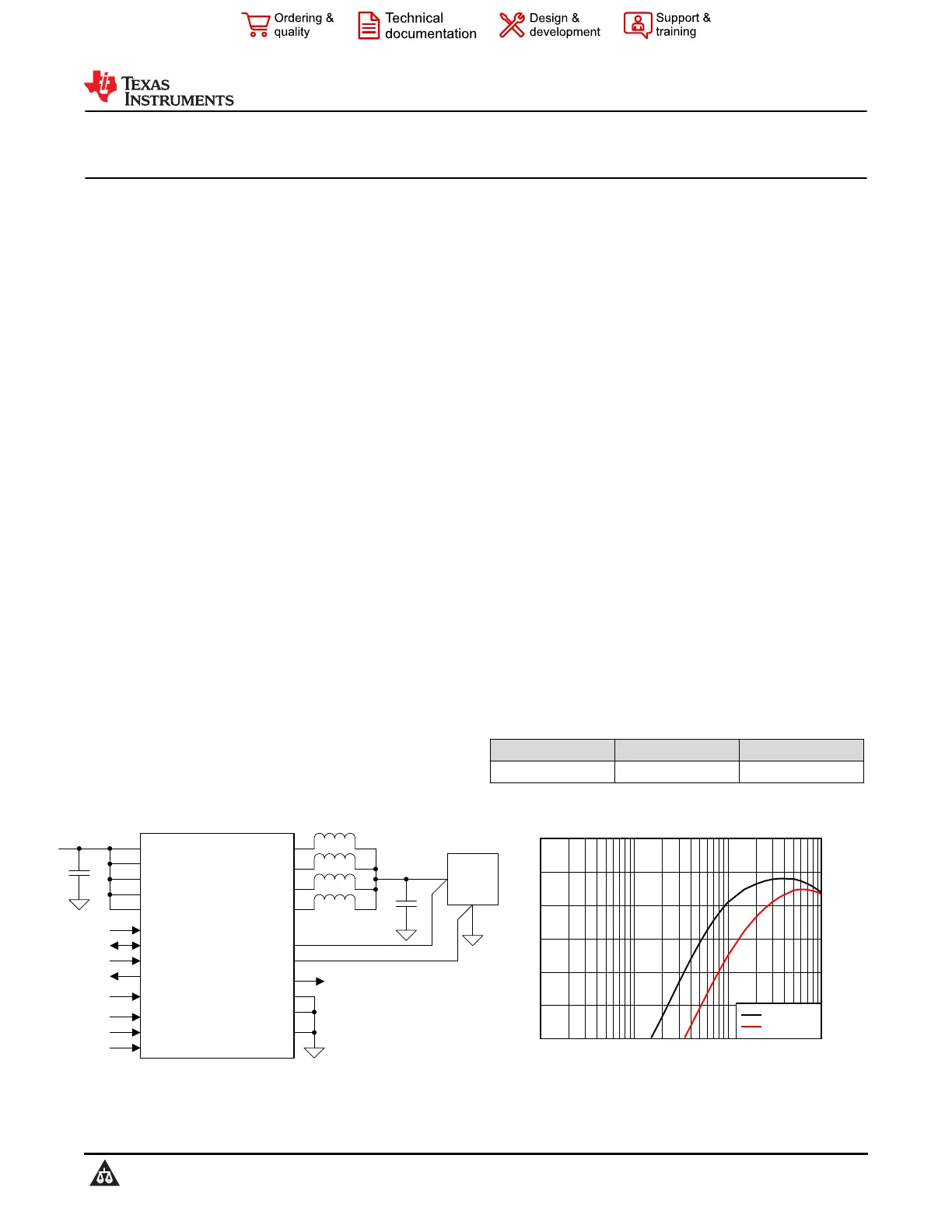
SW_B0
SW_B1
SW_B2
SW_B3
VIN_B0
VIN_B1
VIN_B2
VIN_B3
VANA
V
IN
FB_B0
FB_B1
V
OUT
LOAD
FB_B2
FB_B3
NRST
SDA
SCL
nINT
CLKIN
GNDs
EN1 (GPIO1)
EN2 (GPIO2)
EN3 (GPIO3)
PGOOD
Copyright © 2017, Texas Instruments Incorporated
Simplified Schematic
Current (A)
Efficiency (%)
0.010.1110
40
50
60
70
80
90
100
D140
V
IN
= 3.3 V
V
IN
= 5.0 V
Efficiency vs Output Current
LP875701-Q1
SNVSA05A – DECEMBER 2019 – REVISED AUGUST 2021
An IMPORTANT NOTICE at the end of this data sheet addresses availability, warranty, changes, use in safety-critical applications,
intellectual property matters and other important disclaimers. PRODUCTION DATA.
Produktspecifikationer
| Varumärke: | Texas Instruments |
| Kategori: | ej kategoriserat |
| Modell: | LP875701-Q1 |
Behöver du hjälp?
Om du behöver hjälp med Texas Instruments LP875701-Q1 ställ en fråga nedan och andra användare kommer att svara dig
ej kategoriserat Texas Instruments Manualer

3 April 2026
31 Mars 2026
5 Mars 2026
5 Mars 2026
5 Mars 2026
5 Mars 2026
5 Mars 2026
5 Mars 2026
5 Mars 2026
5 Mars 2026
ej kategoriserat Manualer
Nyaste ej kategoriserat Manualer
3 April 2026
3 April 2026
3 April 2026
3 April 2026
3 April 2026
3 April 2026
3 April 2026
3 April 2026
3 April 2026